
Logic gates are an essential component of digital electronics and are used to handle binary data. Because of its universal nature, the NAND gate is particularly significant among these gates. This article explores the use of NAND gates to implement an OR gate, demonstrating the adaptability and usefulness of these fundamental building blocks.
In this Article, We will be going through the implementation of the OR Gate from the NAND Gate, First We will start our article with the introduction of the OR gate and NAND gate with their Expressions, Logic Diagrams, and Truth Table, Then we will See How We Can Implement OR Gate from NAND Gate, At last, we will conclude our Article with some FAQs.
Table of Content
A basic logic gate known as an OR gate generates an output signal whenever at least one of its inputs is high. The OR gate is symbolically represented as “+” or “1”. Its truth table indicates that if any input is high, it will output a high signal (1); otherwise, it will produce a low signal (0).
The output expression of the OR gate is provided by, if Y is the output variable and A and B are the input variables.
where the OR operation is denoted by the ‘+’ symbol. It reads as follows: Y equals to A OR B.
One of the universal logic gate is the NAND gate , which only generates an output signal when each and every one of its inputs is low. With its symbol “⊼”, the truth table of the NAND gate shows that it outputs a high signal (1) in the absence of a low signal (0) when all inputs are high.
As input NAND Gate takes boolean values and returns:
The NAND gate’s output is determined by, if A, B, and Y are its input and output variables, respectively.

The Implementation of OR Gate from NAND Gate is executed by using De Morgan’s theorem , which asserts that the complement of the AND operation is equivalent to the NAND operation, so that it can be used to construct an OR gate by using NAND gates. So that We can effectively execute the functionality of an OR gate by combining numerous NAND gates in a particular arrangement. So that we can implement an OR Gate by using NAND Gates.
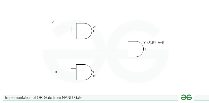
Implementation of OR Gate from NAND Gate
To realize the OR gate from NAND gate, we first complement the inputs A and B. This is done by the NAND Gate in the above Figure. Then, these complemented inputs, i.e. A’ and B’ are applied to a NAND Gate. Thus, we get,
In conclusion, the versatility and applicability of logic gates in digital circuit design are demonstrated by the construction of an OR gate using NAND gates. It is essential to comprehend basic gate manipulation in order to design dependable and effective electronic systems. We can learn a great deal about the fundamentals of digital logic design by investigating the construction of an OR gate from NAND gates. This also opens up new avenues for research into more complex circuitry.
In order to build AND, OR, and NOT gates as well as all other fundamental logic gates, NAND gates are regarded as universal gates.
NAND gates are used in the design of intricate digital circuits due to their affordability, adaptability, and simplicity.
Using universal gates, such as NAND gates, to implement logic gates can result in more efficient and complicated circuit designs with fewer components.